Apple's Huge 3nm Chip Orders for iPhone 15 Pro and M3 Macs Helping to Maintain TSMC's Fab Utilization Rates
Apple supplier TSMC is making strides to improve its production capacity for chips based on its cutting-edge 3-nanometer process technology, according to industry sources, which is expected to debut in this year's iPhone 15 Pro and upcoming MacBook models.
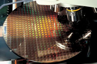
DigiTimes reports that TSMC's 5nm fabrication capacity began to loosen in November 2022 as a result of reduced orders from Apple, amongst other partners, with orders for iPhone chips alone having been slashed by 30%. However, the Taiwanese manufacturer has apparently been able to keep its utilization rate at 70% or higher thanks to Apple's thirst for 3nm:
TSMC continues to improve its capacity utilization for 3nm process technology, which is expected to approach 50% at the end of March, the sources said. The foundry will also grow the process output to 50,000-55,000 wafers monthly in March, with Apple being the main customer.
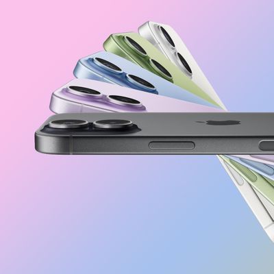
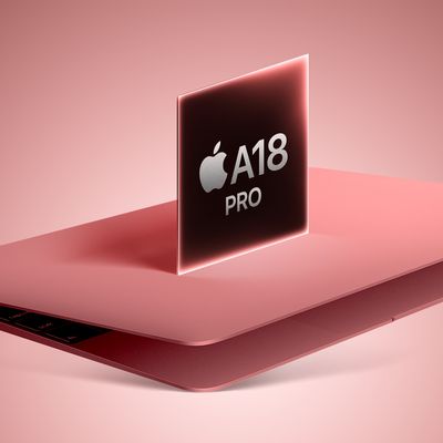
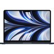
Apple's upcoming iPhone 15 Pro models are expected to feature the A17 Bionic processor, Apple's first iPhone chip based on TSMC's first-generation 3nm process, also known as N3E.
The first-gen 3nm process is said to deliver a 35% power efficiency improvement over TSMC's 5nm-based N4 fabrication process, which was used to make the A16 Bionic chip for the iPhone 14 Pro and Pro Max. The N3 technology will also offer significantly improved performance compared to current chips manufactured on 5nm.
Apple's next-generation 13-inch and 15-inch MacBook Air models are both expected to be equipped with an M3 chip, which is also likely to be manufactured on the 3nm process for further performance and power efficiency improvements. Apple is also reportedly planning to release an updated version of the 13-inch MacBook Pro with an M3 chip. The M2 chip and its higher-end Pro and Max variants are built on TSMC's second-generation 5nm process.
Orders for new AI processors from Nvidia and AMD, as well as Apple's new iPhone chip, are expected to help TSMC avoid further fab utilization declines in the second quarter, DigiTimes' sources said.
Popular Stories
Apple is not expected to release a standard iPhone 18 model this year, according to a growing number of reports that suggest the company is planning a significant change to its long-standing annual iPhone launch cycle.
Despite the immense success of the iPhone 17 in 2025, the iPhone 18 is not expected to arrive until the spring of 2027, leaving the iPhone 17 in the lineup as the latest...
Language learning app Duolingo has apparently been using the iPhone's Live Activity feature to display ads on the Lock Screen and the Dynamic Island, which violates Apple's design guidelines.
According to multiple reports on Reddit, the Duolingo app has been displaying an ad for a "Super offer," which is Duolingo's paid subscription option.
Apple's guidelines for Live Activity state that...
Apple is planning to release a low-cost MacBook in 2026, which will apparently compete with more affordable Chromebooks and Windows PCs. Apple's most affordable Mac right now is the $999 MacBook Air, and the upcoming low-cost MacBook is expected to be cheaper. Here's what we know about the low-cost MacBook so far.
Size
Rumors suggest the low-cost MacBook will have a display that's around 13 ...
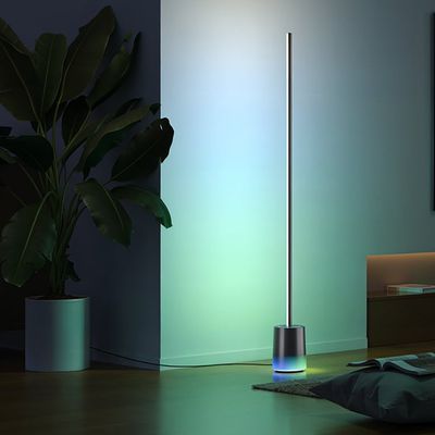
Govee today introduced three new HomeKit-compatible lighting products, including the Govee Floor Lamp 3, the Govee Ceiling Light Ultra, and the Govee Sky Ceiling Light.
The Govee Floor Lamp 3 is the successor to the Floor Lamp 2, and it offers Matter integration with the option to connect to HomeKit. The Floor Lamp 3 offers an upgraded LuminBlend+ lighting system that can reproduce 281...
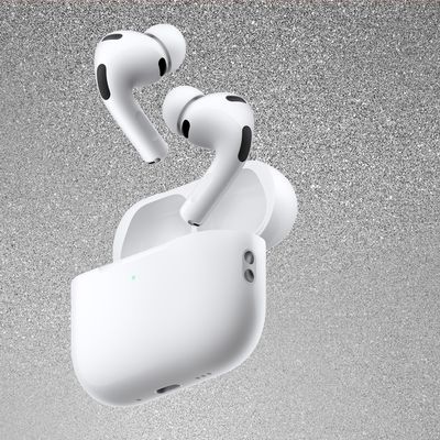
Now that the calendar has flipped over into January, steep discounts on popular Apple products have become more rare after the holidays. However, if you didn't get a new pair of AirPods recently and are looking for a model on sale, Amazon does have a few solid second-best prices this week.
Note: MacRumors is an affiliate partner with some of these vendors. When you click a link and make a...
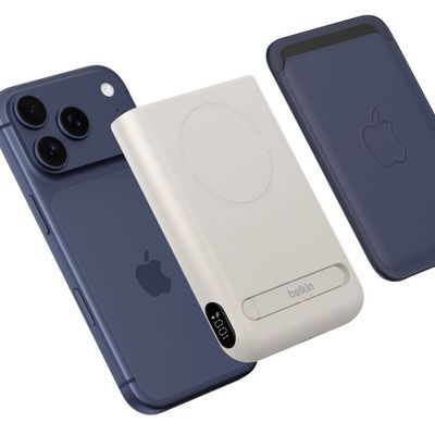
Belkin today announced a range of new charging and connectivity accessories at CES 2026, expanding its portfolio of products aimed at Apple device users.
UltraCharge Pro Power Bank 10K with Magnetic Ring
The lineup includes new Qi2 and Qi2.2 wireless chargers, magnetic power banks, a high-capacity laptop battery, and USB-C productivity accessories, with an emphasis on higher charging...
Apple plans to introduce a 12.9-inch MacBook in spring 2026, according to TrendForce.
In a press release this week, the Taiwanese research firm said this MacBook will be aimed at the entry-level to mid-range market, with "competitive pricing."
TrendForce did not share any further details about this MacBook, but the information that it shared lines up with several rumors about a more...
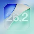
With the release of iPadOS 26.2 and macOS Tahoe 26.2, Apple has improved the Wi-Fi speeds for select Macs and iPads that support Wi-Fi 6E. Updated Wi-Fi connectivity specifications are listed in Apple's platform deployment guide.
The M4 iPad Pro models, M3 iPad Air models, A17 Pro iPad mini, M2 to M5 MacBook Pro models, M2, M3, and M4 MacBook Air models, and other Wi-Fi 6E Macs and iPads now ...