Apple's persistent quest for better performance, longer battery life, and slimmer form factors appears to be driving its research into advanced chip packaging technologies. So-called "2.5D" and "3D" packaging methods stand to offer significant gains in all of these areas by increasing memory bandwidth, reducing power consumption, and freeing up space for higher-capacity batteries.
Apple has been an aggressive adopter of new device packaging methods, mostly thanks to integrated fan-out (InFO) innovations provided by foundry partner TSMC. TSMC's success has spurred it into further developing and diversifying its packaging offerings, and TSMC has emerged as an industry leader in packaging techniques.
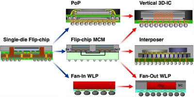
While versions of TSMC's InFO packaging have brought performance improvements to Apple devices, such as better thermal management and improved package height, it has largely not been a direct enabler of improved electrical performance. This is set to change with future packaging techniques and is already seen in some products that utilize interposers for higher density interconnects to on-package memory, such as High Bandwidth Memory (HBM).
The primary memory candidate for inclusion in such a package would be conforming to the Wide I/O set of standards described by JEDEC, and mentioned by name in several of the patents. This memory improves on LPDDR4 by increasing the number of channels and reducing the transfer speed per channel, thus increasing the overall bandwidth but lowering the energy required per bit.
Interposers do, however, pose several issues for mobile devices. Significantly, they introduce another vertical element to the package, increasing total height. Interposers must also be fabricated on silicon wafers just like active ICs, with their dimensions driven by the footprint of all devices that need to be included in the package. These solutions are typically termed as "2.5D" due to some components being placed laterally with respect to one another rather a true stacking of chips.
Rather than adopt interposers for its products as a next step in advanced packaging, the direction of Apple's focus, according to several patent applications [1][2][3][4], appears to be on true "3D" techniques, with logic die such as memory being placed directly on top of an active SoC. Additionally, a patent application from TSMC seems to suggest a level of coordination between Apple and TSMC in these efforts.
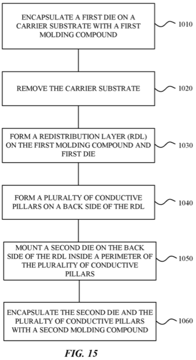
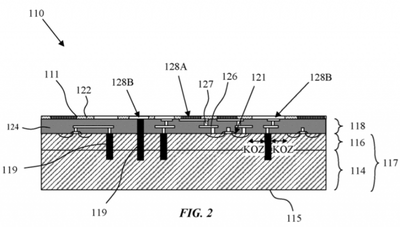
The process has similarities to the existing InFO techniques in that they both involve a redistribution layer (RDL) where contacts on a logic die are routed inside a molding compound with the help of vias directly in the molding compound. Where the 3D process diverts from this is that there is now RDL content on both sides of the die, necessitating the use of through-silicon vias (TSV) directly in the logic die so that interconnections can be made with the top of the die. A key feature of these RDL layers is that interconnect pitches finer than available substrate or interposer types is possible.
Subsequent dies could then be attached to the molding compound, mating with the vias and RDL placed in the previous step. This step could be done multiple times, provided each stacked component has TSVs for the next level of integration, and this is already seen in HBM, which allows for the stacking of up to eight DRAM dies.
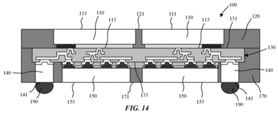
Still, this approach has many technical challenges that have prevented its commercialization. TSVs are expensive to implement and are a serious yield detractor to ICs. Electrical isolation from nearby components' radiated energy can also be a concern, particularly when integrating RF and analog components in a package with other components that would have been separated by space and EMI shielding before. Apple describes techniques to incorporate shielding directly in the package to mitigate this.
This approach also presents thermal challenges since active dies become so closely coupled in mediums that have poor thermal conductivity and shared thermal paths. These concerns extend not only to normal device usage, but also the package integration and any solder reflow steps. Thermal stresses can induce warpage of the packaging components due to differing coefficients of thermal expansion (CTE) amongst the materials utilized in the package. This warpage can lead to broken or separated contacts, resulting in device failure.
The use of a carrier substrate in the process flow mitigates some of the thermal concerns. The direct integration of heatsinks into device packaging is also addressed at various levels of the package assembly, such that higher dissipating die, such as a SoC featuring CPU and GPU cores, could be placed on the bottom of the stack or at a higher level of integration, providing stackup flexibility not seen in previous PoP arrangements.
Embodiments may be applied in applications such as, and not limited to, low power and/or high I/O width memory architecture. Embodiments can enable a short double data rate (DDR) channel to neighboring function units (e.g. SOC, chipsets, etc.) by using RDL and direct chip attach. Embodiments may be particularly applicable for mobile applications that require low power DDR at target performance including high speed and I/O width.
The benefits of the methods described are many. The use of higher bandwidth memory will yield performance improvements. The flexibility of component placement shortens the distance between connected active and passive devices, either lowering the energy required to communicate between them, or reducing parasitic effects that can cause unwanted power loss or dynamic performance degradation. The most notable tasks that stand to benefit are gaming and image processing tasks, which often require large amounts of bandwidth over short time intervals.
Apple Watch Implications
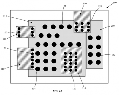
These enhancements would be applicable to all of Apple's mobile devices, but multiple patent applications specifically mention methods of multiple components married together in a System in Package (SiP), as seen in the current Apple Watch. The methods described below are an enhancement on the existing SiP solutions found in Apple Watch in that they introduce true 3D stacking elements enabled by both TSV and Through Oxide Vias (TOV).
In one aspect, embodiments describe system on chip (SoC) die portioning and/or die splitting within an SiP structure (e.g. 3D memory package) in which IP cores such as CPU, GPU, IO, DRAM, SRAM, cache, ESD, power management, and integrated passives may be freely segregated throughout the package, while also mitigating total z-height of the package.
Additionally, the patent describes TSV and TOV pitch in explicit detail, suggesting that keeping package heights down allows them to create very small width vias, with the TOV forming interconnect rows at sizes smaller than even the TSVs. The effect of TSVs stressing active parts of the die, including hurting transistor performance, is also discussed, and the reduced pitches help to mitigate this.
Inclusion of RF transceivers and active devices on substrate types not currently used in Apple mobile devices are covered, indicating all types of active and passive components found in Apple Watch products could be housed in the SiP proposed.
Timeline
Packages featuring 2.5D and 3D connected components have been in consumer devices for several years, but most of the methods described above have yet to debut in mobile devices. The steps described are set to increase manufacturing complexity, and cost and throughput will likely suffer as a result.
Due to cost and yield concerns, a primary candidate for first inclusion of these methods would be a high-margin, low-quantity device. While the iPhone is the highest margin of Apple's mobile products, it is also the largest volume category, with a huge initial demand for each generation. The iPad Pro is a good candidate because of its low volume nature and its classification as a high-performance device. The inclusion of 120Hz refresh rate is something that will benefit from increased memory bandwidth, specifically.
The focus of many of these patents seems to be specifically on SiP methods seen in Apple Watch internals. The Apple Watch is a lower-volume device, and it stands to benefit because its internals are extremely sensitive to package size given the importance of its form factor and battery size. It seems reasonable to expect some of the methods described to be incorporated as soon as the next revision of the Apple Watch, and more progressively in future revisions.