TSMC Details Technology Roadmap With Multiple Offerings to Benefit Future Apple Devices

As part of its recent Q1 earnings call, TSMC announced that its 7-nanometer FinFET process node has entered into high volume manufacturing (HVM), meaning we could see consumer devices featuring the process as soon as the second half of this year.

Previous reports indicated that TSMC is expected to have sole production responsibility for Apple's upcoming A12 chip and its variants expected to debut in new iPhone and iPad products starting this fall. The 7nm node (referred to as CLN7FF, 7FF, or simply N7) is expected to have an approximate 40 percent power and area benefit over TSMC's 10nm FinFET process, utilized in Apple's A11 processors.

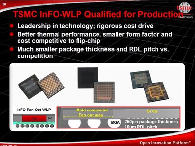
Additionally, as reported by EETimes, TSMC has offered insight into its technology roadmap, both for its silicon processes and for its device packaging technologies. TSMC is believed to have wrested sole ownership of production for Apple's processors away from the dual-sourcing arrangement with Samsung due to its advancements in wafer-level packaging. (What also went largely unnoticed at the time was TSMC's introduction of land-side capacitors attached directly to the substrate.)

Building on the packaging leadership established with its InFO packaging offerings, TSMC has now announced six new packaging types aimed at a variety of devices and applications.

tsmc info wlp slide

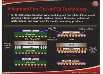
The InFO technique is getting four cousins. Info-MS, for memory substrate, packs an SoC and HBM on a 1x reticle substrate with a 2 x 2-micron redistribution layer and will be qualified in September.

InFO-oS has a backside RDL pitch better matched to DRAM and is ready now. A multi-stacking option called MUST puts one or two chips on top of another larger one linked through an interposer at the base of the stack.

Finally, InFO-AIP stands for antenna-in-package, sporting a 10% smaller form factor and 40% higher gain. It targets designs such as front-end modules for 5G basebands.

But that’s not all. TSMC introduced two wholly new packaging options. A wafer-on-wafer pack (WoW) directly bonds up to three dice. It was released last week, but users need to ensure that their EDA flows support the bonding technique. It will get EMI support in June.

Finally, the foundry roughly described something that it called system-on-integrated-chips (SoICs) using less than 10-micron interconnects to link two dice, but details are still sketchy for the technique to be released sometime next year. It targets apps from mobile to high-performance computing and can connect dice made in different nodes, suggesting it may be a form of system-in-package.

The announcement of these packaging technologies is important because they will enable a variety of different package and interconnect structures for Apple's SoCs, with the immediate benefit being novel interfaces to in-package memory. While InFO offers height, performance and thermal advantages for Apple, they still must interconnect to the RAM seated on top of the application processor through the use of wire bonds in a package-on-package configuration.

This interface presents thermal challenges and limits the width and speed of the memory bus interface due to the type of interconnects. The IC industry has seen quite a bit of effort into novel memory technologies such as High Bandwidth Memory (HBM), but this technology has largely been relegated to graphics processors aimed at scientific, research, and extreme enthusiast use due to the high cost and low yield associated with the silicon interposers that enable the chip-to-memory connections. The fact that TSMC has unveiled a variant of InFO directly aimed at this solution bodes well for its increased adoption in the industry in a variety of products.

The InFO-oS process is of much more near-term interest for mobile device makers such as Apple, where the memory bus widths would be much lower, but the per-pin bandwidth is much higher, as seen in LPDDR4. According to a TSMC report, the "oS" portion this technology refers to on-substrate, where die-partitioning would take place.

This would seem to allow for a 2.5D solution where the memory die is placed alongside the processor die as opposed to suspended above via a mold compound as seen in the original InFO-WLP packaging, enabling the higher interconnect density. However, the retention of a redistribution layer means a mold compound must still be in play, so a more thorough technical disclosure could help eliminate some of the ambiguity with this naming convention. While this would eliminate die-stacking, it would increase the total footprint of the packaged solution, which would still be a concern in a size-constrained mobile package.

TSMC InFO jpg

TSMC InFO variants

While Apple could eventually move to an HBM solution, which affords much greater memory bandwidth at lower power levels, the wafer-on-wafer (WoW) announcement is a genuine step towards true 3D integrated circuits, where eventually dies would be stacked directly on top of each other and interconnected through vias placed directly in the IC die.

The innovation for TSMC here would be in exactly how it packages these dies together, and what the interfaces look like as well as what type of redistribution layers (RDLs) they offer. While not directly applicable to Apple's line of processors, the InFO-AIP is also an important development, as radio frequency (RF) front-ends stand to take on another order of complexity with their adoption of much wider frequency bandwidths needed for 5G standards.

Beyond the 7nm node, TSMC also shared its outlook for the foundry's successive nodes, 7nm+ and 5nm. 7nm+ will be TSMC's first node to feature extreme ultraviolet (EUV) lithography, which stands to simplify the mask process by eliminating the need for multiple patterning in many areas to define smaller features.

Following 7nm+ will be 5nm, which would enter risk production late next year if current timelines hold, meaning volume production would occur sometime in 2020, though likely too late for a fall 2020 product launch, even with the most optimistic timelines. Though EUV has been long-awaited and will solve many problems in the industry, it brings a host of its own issues and will not bring huge performance jumps in successive nodes, nor will it grant smoother node transitions, as 5nm already presents its own EUV challenges.

The node delivers 35% more speed or uses 65% less power and sports a 3x gain in routed gate density. By contrast, the N7+ node with EUV will only deliver 20% more density, 10% less power, and apparently no speed gains — and those advances require use of new standard cells.

Still, the above news is encouraging, as Apple should be able to enjoy the benefits of a new technology node for at least two out of the next three years. This will offer a boost as its processor architecture gains slow down, and the advent of new packaging techniques will allow Apple to overcome bandwidth and thermal constraints in ways that were simply not possible before.

TSMC has also offered hope for the future, painting the picture beyond 5nm in broad strokes with plans for newer transistor topologies such as silicon nanowires, and moving beyond silicon as the prime semiconducting medium to materials that ultimately offer higher carrier (electrons and holes) mobility.

TSMC also detailed ways to improve the conductivity and reduce the parasitics associated with the interconnects present in the silicon die. Ultimately, these interconnects often dictate how quickly transistors can switch due to the effective line load on them, and that is a concern all the way from the die to the package and on to the PCB. TSMC seems to be diligently pursuing a variety of solutions for its customers on two of those fronts, and its packaging solutions are bringing more and more of those PCB components straight into the device package to combat the third element.

Tags: A12, TSMC

Popular Stories

iPhone 17 Pro Render Front Page Tech

iPhone 17 Pro Launching Later This Year With These 8 New Features

Tuesday March 4, 2025 3:15 pm PST by
While the iPhone 17 Pro and iPhone 17 Pro Max are not expected to launch until September, there are already plenty of rumors about the devices. iPhone 17 Pro's alleged design via Front Page Tech Below, we recap key changes rumored for the iPhone 17 Pro models as of March 2025: Aluminum frame: iPhone 17 Pro models are rumored to have an aluminum frame, whereas the iPhone 15 Pro and iPhone...
iPhone 16 Pro vs iPhone 17 Air Feature

iPhone 17 Air and 17 Pro Max Allegedly Same Size Apart From Thickness

Friday March 7, 2025 2:45 am PST by
Apple's all-new ultra-thin iPhone 17 Air shares the same dimensions as the iPhone 17 Pro Max, with the only difference being in the thickness of the devices, according to the leaker Ice Universe. Posting to their Weibo account, the Chinese leaker today claimed that the iPhone 17 Air and iPhone 17 Pro Max have identical body length, width, screen size, and bezels. "The only difference is the...
Apple Intelligence General Feature

Apple Delays Apple Intelligence Siri Features

Friday March 7, 2025 9:35 am PST by
Apple is delaying some of the Apple Intelligence Siri features that it expected to release in iOS 18, an Apple spokesperson said in a statement to Daring Fireball. Apple says that it is going to take longer than expected to roll out the more personalized Siri experience, and that these features will be rolled out "in the coming year.""Siri helps our users find what they need and get things...
Apple MacBook Air hero

Apple Says New MacBook Air Up to 23x Faster Than Intel-Based Model, But Read the Fine Print

Thursday March 6, 2025 1:46 pm PST by
Apple has a staggering marketing claim for the new MacBook Air with the M4 chip. Specifically, Apple says the new MacBook Air is up to 23x faster than the last Intel-based model. However, there are some details in the fine print to be aware of. First, Apple said it compared a new 2025 MacBook Air with a 10-core M4 chip and 32GB of RAM to a 2020 MacBook Air with a quad-core Intel Core i7...
iphone 17 pro asherdipps

iPhone 17 Pro Max Said to Be Thicker to Accommodate Larger Battery

Friday March 7, 2025 2:47 am PST by
Apple has increased the thickness of the upcoming iPhone 17 Pro Max compared to the current generation iPhone 16 Pro Max, claims the Chinese leaker known as Ice Universe. Apple is said to have increased the depth of the iPhone 17 Pro Max to 8.725mm, up from 8.25mm on the iPhone 16 Pro Max, which would be a 0.475mm difference in thickness. The increase "surely means a larger battery,"...
Apple MacBook Air hero

New MacBook Air Quietly Fixes This Decades-Long Design Oversight

Friday March 7, 2025 6:58 am PST by
In a move that probably won't make headlines but should delight detail-oriented Mac users everywhere, Apple has quietly corrected a 26-year-old design inconsistency on its keyboards. The Mute key, a staple on Mac keyboards since the PowerBook G3 'Lombard' debuted in 1999, has finally received a logical redesign on the new MacBook Air with M4 chip. As spotted by iCulture, the key now displays ...
ipad air magic keyboard feature

Everything Apple Announced This Week

Wednesday March 5, 2025 4:03 pm PST by
It's been a busy week for Apple, with new products announced on Tuesday and Wednesday. We're now caught up on what's been rumored for a spring launch, so we thought we'd recap everything Apple came out with this week. Subscribe to the MacRumors YouTube channel for more videos. iPad Air Apple updated the iPad Air on Tuesday, updating it with the new M3 chip. The iPad Air still comes in...
2016 12 inch macbook feature

Apple Introduced Its Most Controversial MacBook 10 Years Ago Today

Sunday March 9, 2025 1:00 am PST by
Apple announced the infamous 12-inch Retina MacBook a decade ago today, an experimental new Mac that was as controversial as it was revolutionary. Apple unveiled the 12-inch MacBook on March 9, 2015, at the "Spring Forward" event in San Francisco, California. The event was primarily focused on the Apple Watch, which was being fully detailed ahead of its launch the following month, so the...
Apple Summer 2025 Feature 1

Here Are the New Apple Products We're Expecting This Summer

Friday March 7, 2025 7:09 am PST by
Now that Apple has announced its new more affordable iPhone 16e, and new MacBook Air and Mac Studio models with M4 and M3 Ultra chips, we thought we'd provide a quick recap of what else we are expecting from the company in the summer months ahead. There are at least three product categories that we are hoping to see some movement in before summer is over, but of course, nothing is...

Top Rated Comments

chrmjenkins Avatar
89 months ago
Samsung announced 4nm about this time last year. Here's one article ('https://www.tomshardware.com/news/samsung-4nm-foundry-roadmap-revealed,34515.html') about it. Of course, we all know that their nm is not as good as Apples- er- TSMCs nm (until Apple might choose to go with Samsung again, and then they are fine).;)

I think I saw something about somebody working on 3nm but I don't remember that very well.

I've long been under the impression that reliability starts becoming an increasingly big problem much smaller than this. Unless something has changed, I suspect the "true 3D ICs" part of the article may be the bigger deal.

However, I'm no expert on this topic, and did not stay at a Holiday Inn Express last night either.;)

Perhaps someone much more knowledgable is up to date on where Moore's Law and this limit is currently believed to be maxed (or is that min'd) out???
No roadmaps go beyond 3nm. The trouble, aside from increasing manufacturing challenges, is that quantum effects start to dominate and the transistors don’t behave like they used to at larger geometries. Modern transistor modes have hundreds of device parameters that attempt to track all the relevant physical parameters that affect their performance on modern nodes.

The width of a silicon atom is 0.2 nanometers, so we are talking transistors with features in the tens of atoms already. There is a real physical limit, even if the quantum effects weren’t in play. This is why there are efforts to find a replacement for silicon that allows circuits to switch faster. There are already materials out there, but they cannot be manufactured on the same scale and density as the current CMOS processes.

3DIC techniques tackle it from the energy per bit angle by making the interconnects closer together, making them easier to drive between interfaces, and thus, able to drive faster. Thermal management techniques will also help because heat has a negative influence on transistor performance, and thus, speed.
Score: 17 Votes (Like | Disagree)
wizard Avatar
89 months ago
Nice reporting!! Seriously Macrumors should be applauded for this article.

As for Apple it would be nice to hear that the iPad in getting a 7nm version of the A11, A11X in Apples naming scheme. I know it would not be "normal" practice at Apple but iPad is relatively low volume allowing TSMC to ramp up the production at this node. Lets face it a 40% improvement would be amazing.
Score: 13 Votes (Like | Disagree)
luvbug Avatar
89 months ago
TMSC's chip technology certainly is impressive- but odds are pretty much 100% that the new iPhone XI with the new A12 TSMC chip running iOS 12 will lag & stutter anyway. Sigh.
And your basis for saying that is ... ?
Score: 9 Votes (Like | Disagree)
gaximus Avatar
89 months ago
7nm... 5nm... what happens when they run out of nanometers? :eek:
then picometers
Score: 8 Votes (Like | Disagree)
mozumder Avatar
89 months ago
TSMC is the best foundry in the business.
Score: 5 Votes (Like | Disagree)
chrmjenkins Avatar
89 months ago
This is a crucial point, often lost when some talk about Apple replacing Intel processors next year with A-series.

Yes, Apple has a world class silicon design team, but it isn’t possible to get the performance of Intel 90-140W CPUs just by scaling current A-series processors to 64 or more cores. Certain workloads could utilize that type of multicore processor very efficiently of course, but many times performance is limited by how much work can be done when executing a single thread.

I’d be interested to hear your take on a timeline for Apple to transition to their own CPU.
The most interesting part about Apple transitioning to a custom CPU for Mac OSX products would likely be the extensions they made to the ISA rather than just the architecture. They could add a lot of heavy lifting vector instructions and other desktop class features to really balloon the TDP, but they’d also likely need to make a large number of their own instructions to adapt it to the desktop space. There would also be the question of whether they include a GPU in the design, design their own discrete GPU, or go to AMD or Nvidia for a more traditional route. They recently ceded the mobile GPU performance crown to Qualcomm, so it will be interesting to see how their custom GPUs develop.

I have no questions about their technical capability. They beat the market to 64 bit by a wide margin, have churned out multiple custom designs in the same year across multiple product lines, and have validated a new design to two new foundry processes at once. They simply choose and execute.

Apple is never use the state of the art memory inside of any of it's device. They just wait till memory prices fall and then buy the lowest memory chip set and speed. I think the LPDDR3 and the lowest speed LPDDR4 are neck in neck on pricing. The bandwidth is the primary difference between the two memory components for the most part. More lanes, faster the over all system!
Apple has typically adopted the latest mobile memory standard within a year of it appearing on the market in competing products. They equipped an iPad with a 128 bit off package memory to meet their high bandwidth requirements, which you don’t see with other vendors. They were also the first to really raise the bar for NAND performance in mobile devices. I would say Apple has a history of leadership in memory adoption in the mobile space.
Score: 5 Votes (Like | Disagree)