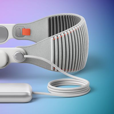
 One of the key challenges for Apple in developing the Apple Watch was figuring out how to maintain acceptable battery life for the device in the face of power-hungry components such as the main processor and display.
With watchOS 3 introduced at WWDC in June, Apple showed off the ability to allow multiple Apple Watch apps to remain active and refresh in the background, acknowledging that its initial approach to managing power and other system resources was conservative but that real-world experience had shown the device could handle more demanding tasks.
In addition to software improvements, future generations of the Apple Watch will need to become more efficient on the hardware level, with new versions of the S1 chip that serves as the brains of the device being a primary target for improvement. With that in mind, we've taken a technical look at what the future could hold for semiconductor technology as it relates to battery-limited devices like the Apple Watch.
As transistors begin to reach their physical size limits in modern semiconductor processes, it becomes more difficult, and thus more expensive, to make them smaller. In addition to the cost per transistor no longer shrinking, it also becomes more difficult to control waste power, or leakage. New transistor geometries such as non-planar "3D" FinFETs are becoming popular to address device leakage, but as wearables such as the Apple Watch have begun generating consumer interest, the gains seen in these semiconductor processes are simply still not enough.
For a wearable device such as the Apple Watch, controlling power usage while the device is idle in standby mode is critical to keeping the overall battery life competitive. The need for ultra low power and cheaper silicon processes that are also performance competitive have made way for transistors made with more traditional lithography techniques with higher substrate costs.
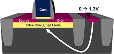
The leading candidate technology of this variety is fully depleted silicon-on-insulator, or FD-SOI. FD-SOI technology innovates on traditional "bulk" transistors (seen in Apple devices prior to and including the A8) in two main ways. The first improvement is that the ultra-thin channel on top of the insulating body eliminates the need to dope the channel with additional positive or negative charge carriers, eliminating a source of device variation which can hurt performance optimization. The second improvement is that the insulating body and other characteristics drastically reduce leakage current.

The additional benefits of this process lie in the ability to dynamically control the transistor switching performance by way of biasing the transistor body. This can also be done in traditional bulk type semiconductors, but at the cost of impacting leakage performance. In the case of FD-SOI transistors, the effect is that the performance of the transistors can be modulated in real time.
Modern chips already feature multiple forms of dynamic frequency and voltage scaling (DVFS), but the ability to control FD-SOI transistors is even greater through the use of forward body biasing. Transistors can be dynamically controlled to switch faster by modulating the amount of voltage that must be applied to the device gate to effectively form a channel to operate the transistor.

This dynamic control between forward and reverse body biasing means that the transistors can be operated at extremely low voltages, near the threshold point. Operating at as little as 0.5V, power use can be drastically reduced as device power is often directly correlated with the square (or cube) of applied voltage.
 The reason this technology is significant for wearables is because the main system on a chip (SoC) can play such a large part of the device's power consumption, particularly when most usage is idle, as shown in the Android-based example to the right. Reviews have shown that the wrong SoC can absolutely kill a smartwatch's battery performance. The other large factor in a smartwatch's battery usage would be the screen - a component where Apple is much more at the direct mercy of its vendors to provide an acceptably performing product.
Rapid design turnaround from Apple's processor groups, in addition to simultaneous launches of the A9 SoC on competing FinFET processes, show that Apple has the technical bandwidth to commit to introducing an additional design process into its mixture. In fact, we know that the original S1 SoC featured in the debut Apple Watch was manufactured on Samsung's 28nm LP process, in contrast to the leading 20nm process which would have been available at the time.
It is not unreasonable to think that Apple could make a somewhat lateral move to adopt Samsung's 28nm FD-SOI process, which is available now. Further down the road is the possibility of a 22nm FD-SOI process, and the technology will no doubt continue to grow if the market proves the demand as time goes along.
FD-SOI also has tremendous promise for analog and RF circuit applications due to its low leakage characteristics. It would not be a surprise to see RF front-end suppliers such as Qualcomm adopt FD-SOI for their modem and multi-band amplifier applications, and should Apple's hiring of engineers with RF expertise ever come to fruition, it would be a suitable candidate for more custom parts directly from Apple. In any event, do not be surprised if analyses of the next Apple Watch have a few surprises in store when the teardown firms get their microscopes out.


