Close on the heels of its iPad mini teardown, iFixit has performed a similar procedure on the fourth-generation iPad. The new iPad is extremely similar to the previous model, with the main exceptions being the move to a more powerful A6X chip and a change to Apple's new Lightning connector.
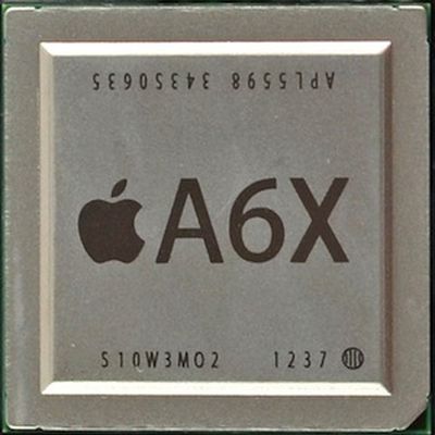
Of most significant interest is of course the A6X chip, which would be an enhanced version of the A6 chip that debuted in the iPhone 5, with improved graphics to help drive the iPad's large Retina display. A date code on the A6X reveals that it was manufactured in the 37th week of 2012, which corresponds to mid-September, but a more detailed analysis of the A6X will need to wait for chip teardown experts such as those at Chipworks to get their hands on the part.
Other interesting discoveries include:
- The display is manufactured by LG, as opposed to the Samsung display found in the third-generation iPad torn down by iFixit. Apple does, however, source many of its components from multiple vendors, so it is unclear whether Apple has excluded Samsung from display production on the fourth-generation iPad.
- The logic board remains the same size as in the previous model, but Apple has tweaked the layout of some of the chips.
- The new Lightning port is housed in a frame that is equal in size to that of the 30-pin dock connector in the previous generation, meaning that Apple has not saved any interior space with the move to the Lightning connector. Apple will, however, almost certainly take advantage of the reduction in space needed for the Lightning connector in a more significant redesign for a future generation.
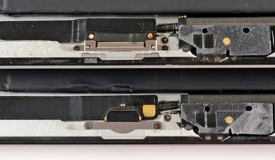
30-pin dock connector from third-generation iPad (top) and Lightning connector from fourth-generation iPad (bottom)
- The improved front-facing camera is slightly thicker than in the previous model, but fits into the same space within the device's body.
- The battery carries the same A1389 part number as in the third-generation iPad.
- Just like in the third-generation iPad, the fourth-generation model contains 1 GB of RAM housed in two Elpida chips separate from the A6X package.
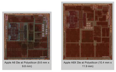
Update: Chipworks has examined the A6X, finding that it is indeed a significant reworking of the A6 found in the iPhone 5, unsurprisingly focused on graphics capabilities.
This is not just an A6 with a couple minor tweaks. The A6 is 94mm2 while the A6X is 123mm2 – a full 30% larger.So where did that extra area go? Well, firstly, it did not go to the CPU core. The A6X uses the identical CPU to the A6. Same size, same layout. This is not surprising given that the prior CPU used custom layout techniques, and therefore it would be a huge amount of work to redesign so soon. Much of the extra area has gone to the GPU cores which are up from 3 to 4. More notable is that each of these GPU cores is much larger.On the A6X each GPU core is 8.7mm2 while the A6 GPU cores are only 5.4mm2. The overall area occupied by the A6X GPU cores is more than double that of the A6!
