Financial news website The Motley Fool has shared details of the A9X die featured in the new Apple iPad Pro, thanks to analysis from electronics teardown firm Chipworks. The photo reveals the A9X's dual-core CPU and a 12-cluster GPU to drive the device's massive display.
While the CPU core count observed in the A9X matches that of the A9 from the iPhone 6s and 6s Plus, the 12-cluster GPU is twice as powerful as the six-cluster GPU found in the A9 design. Otherwise, the core and cluster designs appear to be identical to those found in the A9 die shots.
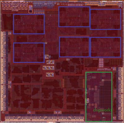
Chipworks confirms that the die shown in the photo is fabricated by TSMC, and it does indeed show similarities with the existing A9 TSMC die already pictured by Chipworks.
The Motley Fool also points out that the 8 MB third level cache featured on the A9 to help manage data flow to and from memory is not present on the A9X die, suggesting that the absence of this cache is due to the increased memory bandwidth that the A9X enjoys by having a memory interface twice the width of the A9 die. Indeed, in the included die shot, an expansive DRAM memory interface can be observed across three sides of the die.
It is also worth mentioning that while the display resolution is much greater than on other iPads, the iPad Pro does not feature the 12-megapixel camera of the iPhone 6s and 6s Plus that would place additional demands on the memory hierarchy for real-time image processing.
The presence of only two CPU cores is also interesting, given that the A8X featured in the iPad Air 2 had three CPU cores. The iPad Pro can make up any resultant performance deficiencies through a combination of higher efficiency, thanks to the new architecture, as well as the large clock speed boost compared to the A8 designs.
Even with the absence of L3 cache and only two CPU cores, the A9X measures 147 square millimeters. This is just 18 square millimeters shy of Apple's largest chip design ever, the A5X featured in the first iPad with retina display. Unsurprisingly, the A5X was quickly phased out and replaced by the smaller A6X seen in the fourth-generation iPad. The A9X's 147 mm^2 die is also larger than the latest quad-core Skylake design from Intel, which comes in at 122 mm^2 on its 14nm FinFET process.
While it may simply be a perfect mixture of die space saving and adequate memory bandwidth for the A9X design, the lack of the third level SRAM cache may tip future design decisions should memory bandwidth improve substantially. 3D IC packaging designs are rapidly approaching mainstream consumer electronics, and they boast a variety of memory configurations, which stand to significantly improve memory bandwidth while also providing lower power dissipation. As we covered recently, packaging technologies enabling these high bandwidth memories may arrive as soon as Apple's A10 SoC for devices next year.


