Since the Apple Watch's initial unveiling last September, Apple has touted the S1 chip that serves as the brains of the device, with the company noting is has essentially packed an entire computer onto a single ultra-compact chip that is encapsulated in resin to help protect it from the elements.
iFixit was unable to delve into the S1 itself in the firm's initial teardown of the Apple Watch, and Chipworks offered an early look at the chip's internals starting x-ray imaging, but now ABI Research has more fully deconstructed the S1 and identified a number of its components.
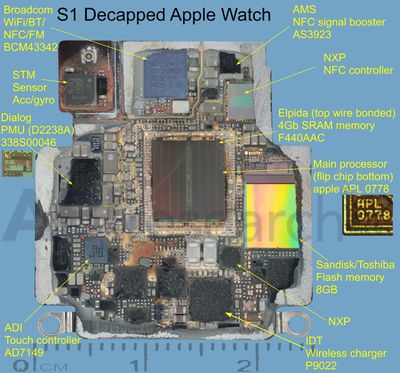
ABI's photo shows the center of the S1 dominated by the main processor carrying part number APL 0778, with 4 Gb (512 MB) of Elpida SRAM on top. We've yet to see a detailed look at the internals of the main processor, which should provide yet another interesting look at a custom Apple chip design when it does surface.
Also included on the S1 are an 8 GB flash storage chip, the Broadcom Wi-Fi chip cleverly identified by Chipworks from Apple's promotional footage last September, an accelerometer/gyroscope from STMicroelectronics rather than the predicted InvenSense, touch controllers unexpectedly from ADI, and a wireless charging chip from IDT to facilitate the Apple Watch's inductive charging.
“The design is an obvious variation from Apple’s smartphones, with many high-end functions / chips included that normally would not be found in a simple watch,” comments Jim Mielke, VP Engineering at ABI Research and head of the TeardownIQ group. “Judging by the complexity of the printed circuit board (PCB), and the number of parts on the PCB, one might think the Apple watch is a full-fledged cellular connected watch but in fact connectivity is limited to Wi-Fi, Bluetooth, and NFC.”
In its initial look last week, Chipworks highlighted the 6-axis accelerometer/gyroscope, which marks the first time Apple has been able to include all of that functionality in a single component.
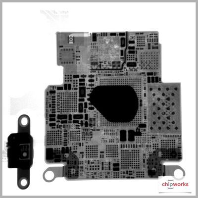
This is the first time that we see a true 6X sensor in an Apple product that doesn’t require an external accelerometer. In the iPhone 6 and 6+ we saw an Invensense 6 axis sensor and a Bosch 3 axis accelerometer. Here in an even more compact design, the Apple Watch, we finally have a solution for all 6 axis in a single component.
As seen in iFixit's teardown, the S1 is a remarkably compact chip taking up a small percentage of the overall device volume in laying flat in the bottom of the casing. The majority of the space inside the casing is taken up by the battery and Taptic Engine/speaker assembly. We expect to see more details on the S1, particularly the main processor, in the coming days as chip experts get closer looks at the part.


